Featured
A variety of images taken using a Veeco Dimension Icon AFM and our SCOUT 350 probes.
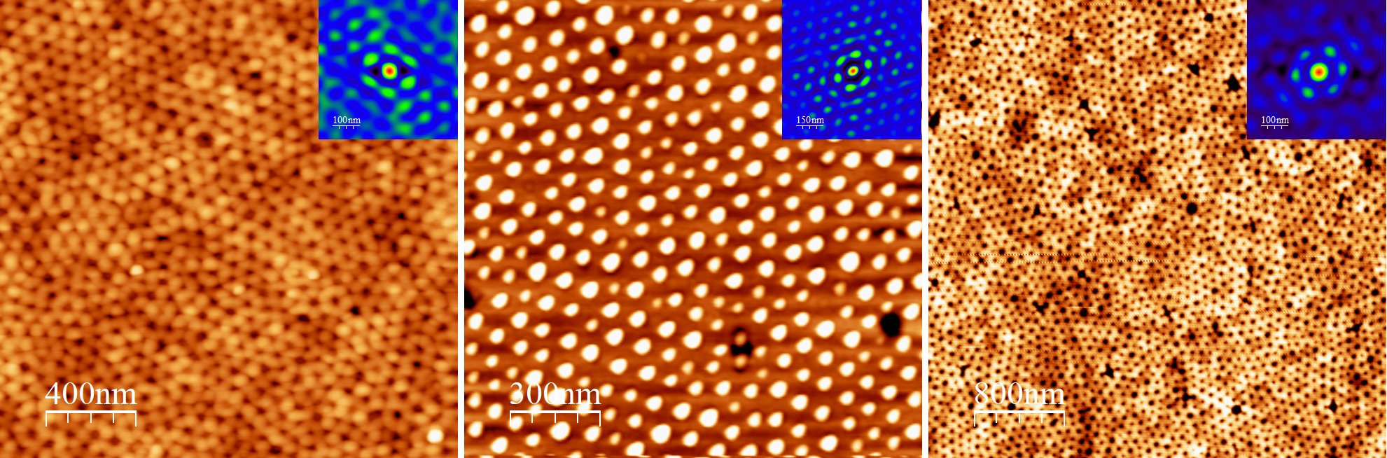
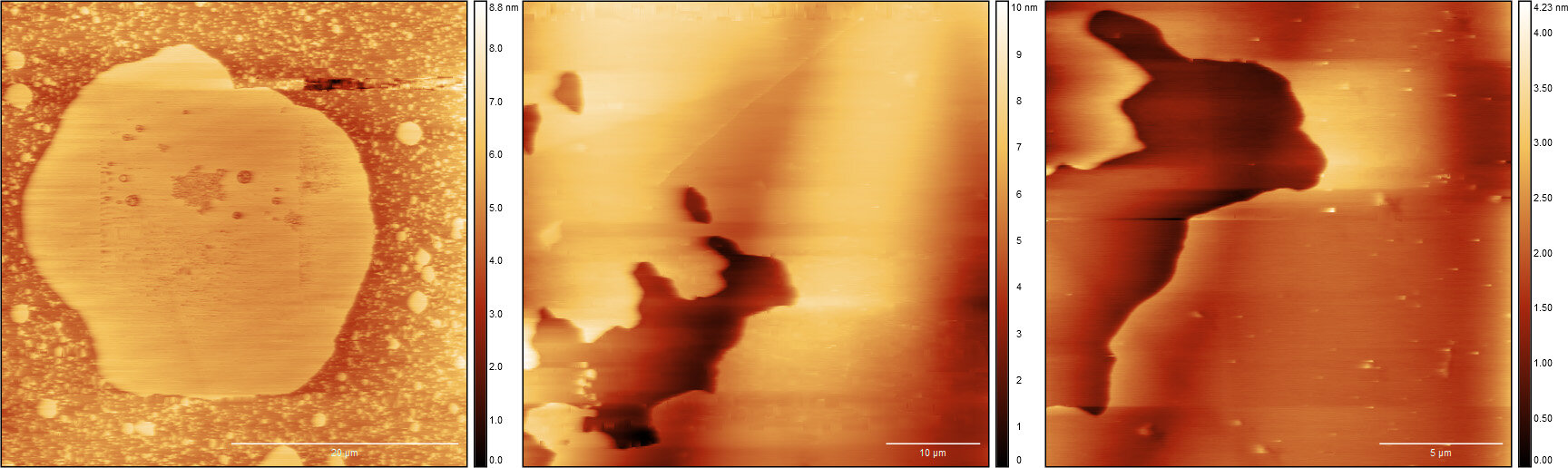
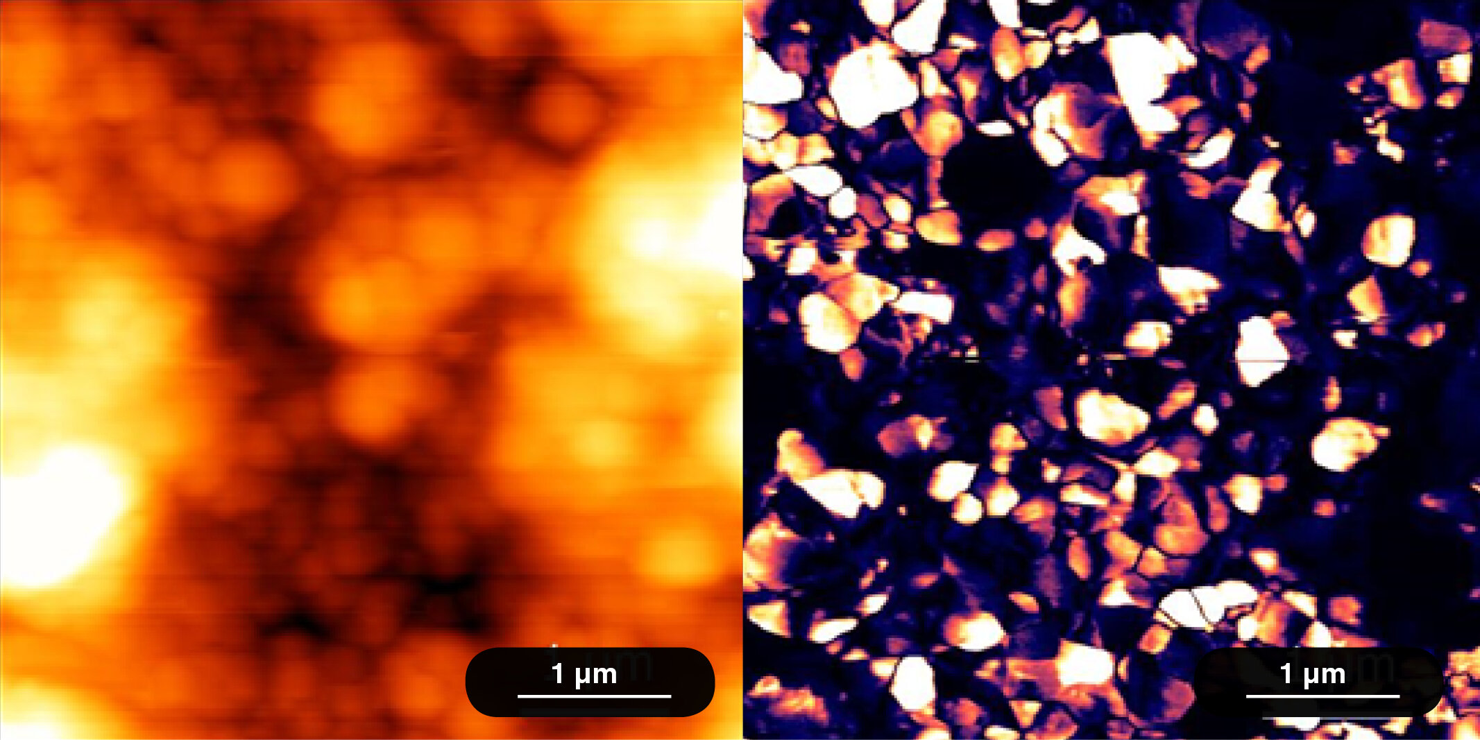
(Left) a mesoporous aluminosilicate thin film made by block copolymer co-assembly. (Middle) a gold nanoparticle array (diameter around 40 nm) created via block copolymer templating. (Right) a mesoporous block copolymer membrane made by block copolymer self-assembly.
Images courtesy of Dr Alberto Alvarez at University College London (UCL).
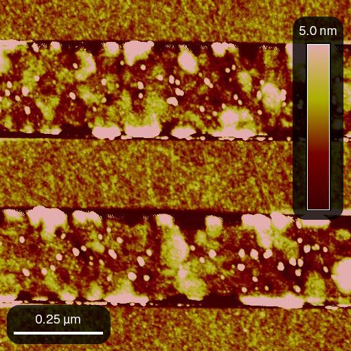
Gold electrodes deposited on an oxidized silicon substrate imaged using our SCOUT 70 RAl probes.
Image courtesy of Prof. Walter Smith from Haverford College.
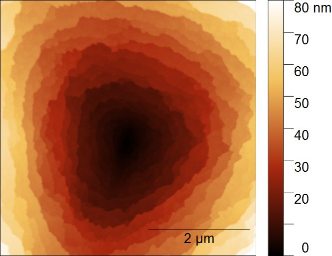
VOx surface imaged using a Cypher ES (Asylum Research) and our SCOUT 70 RAl probes.
Image courtesy of Dr Sergey Luchkin from Skolkovo Institute of Science and Technology.
AM-AFM topography images of Pyr3LPC compounds transferred on mica substrate using a JPK Nanowizard Ultraspeed with our SCOUT 350 RAu. (LPC = lysophosphatidylcholine, Pyr = pyropheophorbide).
Images courtesy of Dr Ali Makky from University of Paris Sud.
A solid supported lipid bilayer on freshly cleaved mica imaged using AC mode buffer and our SCOUT 70 RAl probes. Lipids used include DOPC (1,2-dioleoyl-sn-glycero-3-phosphocholine) and Rhodamine-DOPE (1,2-dioleoyl-sn-glycero-3-phosphoethanolamine). Images show a smaller surface of a lipid bilayer with vesicles and smaller bilayer dots (left) and a larger bilayer surface with a hole (middle and right)
Images courtesy of Dr. Bizan Balzer from Albert-Ludwigs-Universität Freiburg.
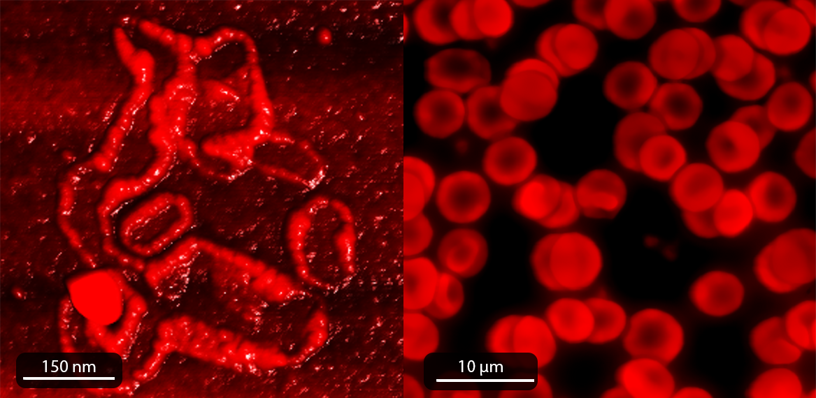
Protein Imaging in Blood from Individuals with Alzheimer’s Disease (left) and Large-Area Imaging of Red Blood Cells (right), using our SCOUT 70 HAR RAu probe on a Multimode 8 (with e-scanner) and Dimension Icon.
Image courtesy of Dr Peter Nirmalraj from EMPA, DOI: 10.1126/sciadv.abj2137.
KPFM Contact Potential Difference Map (left) and Topography (right) of an epitaxial graphene film grown on SiC, showing areas of single-layer (brighter CPD contrast) and bilayer (darker CPD contrast) graphene, using our SPARK 70 Pt probe.
Images courtesy of Dr Francesco Lavini from New York University.
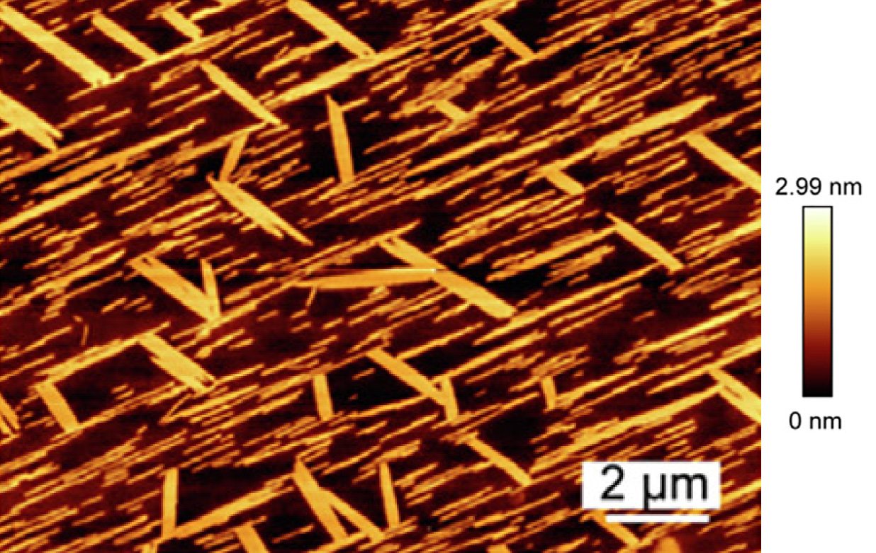
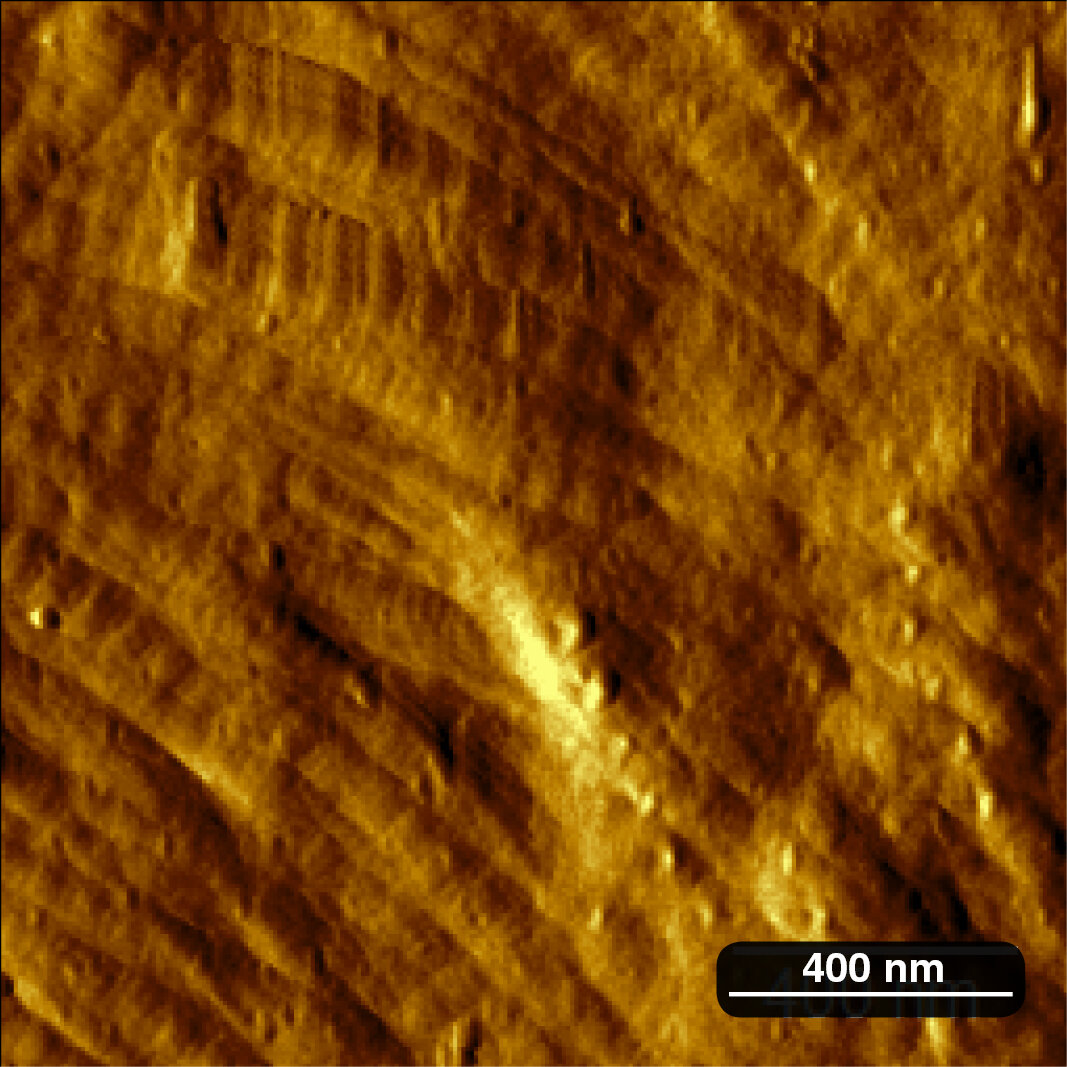
A multiple high-aspect ratio silicon nanowire trace, using our SCOUT 350 HAR RAl probe on a Veeco Dimension 3100 as part of the EMPIR research project Nanowires.
Image courtesy of Dr Walter Knulst from VSL Dutch Metrology Institute.
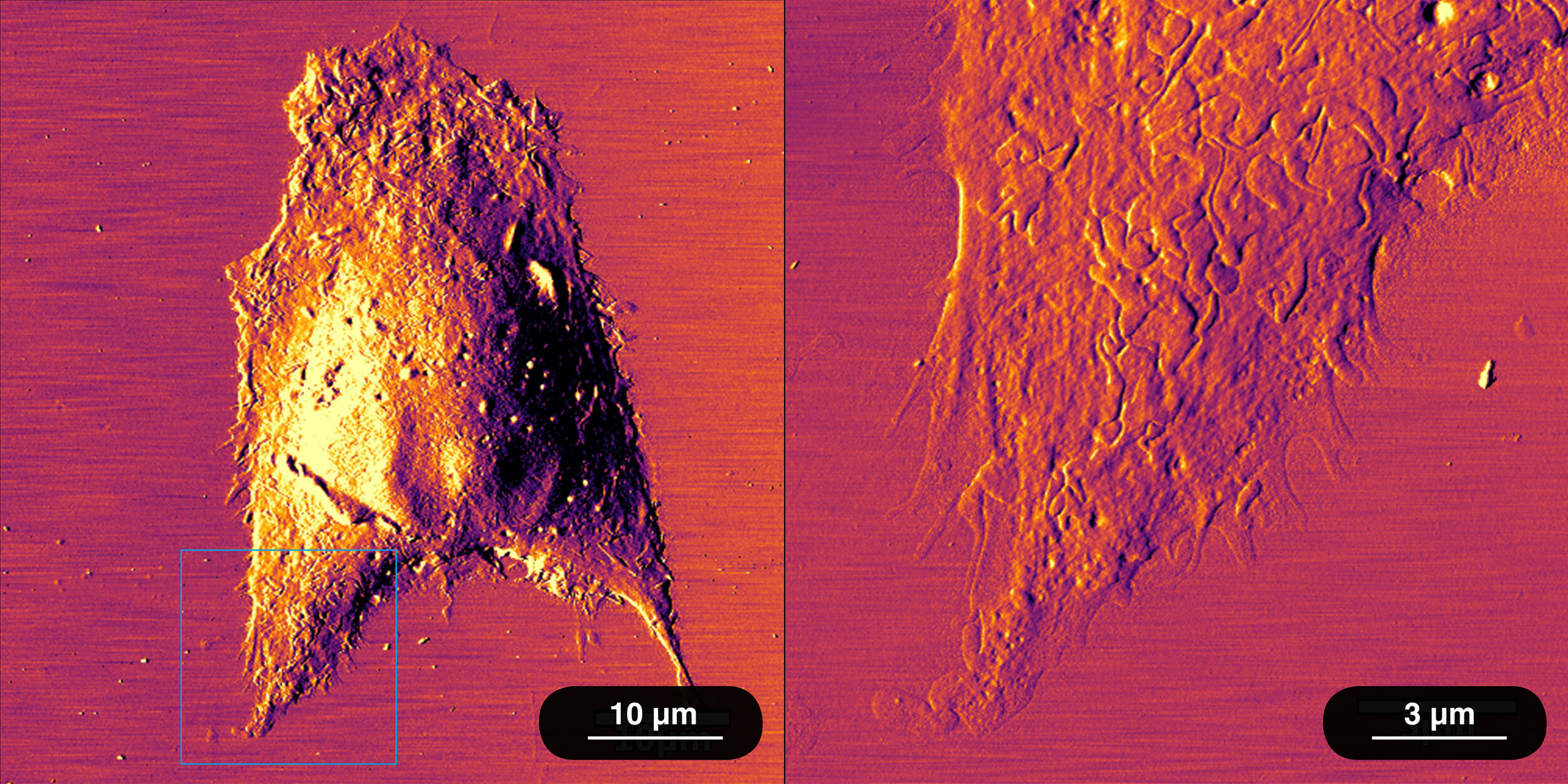
Amplitude image of a HEK293T Cell (Human Kidney) in PBS, using our SCOUT 70 RAl probe on an MFP-3D-BIO AFM (Oxford Instruments).
Image courtesy of Dr Biran Wang from Memorial Sloan-Kettering Cancer Center.
EFM images showing topography (left) and dielectric (right) of a bundle of long SWCNTs covered in surfactant on a Si/SiO2 substrate. Data acquired with a SPARK 350 Pt probe on an Asylum Research MFP-3D Origin AFM.
Images courtesy of Erin Christensen and Todd Krauss, University of Rochester, USA.
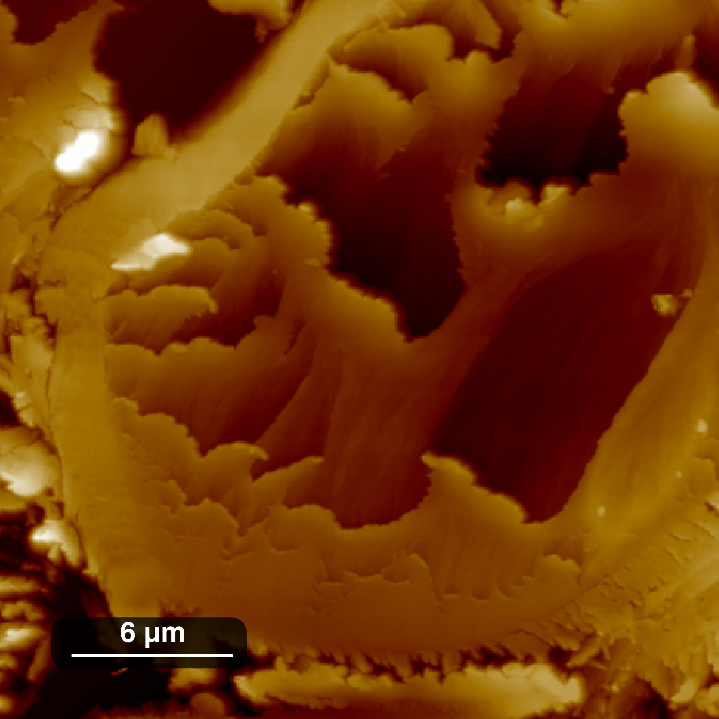
Topographical images of the cell wall and structure of an LR white resin-fixed sample of loblolly pine whitewood (branch from a 23 year old tree) taken using a SCOUT 350 RAl on a Bruker Dimension Icon AFM.
Image courtesy of Ashton Enrriques and Dr Paul Davis from Boise State University, Idaho. Samples provided by Idaho National Laboratory.
Topographical image of amyloid beta (1-42) protein oligomers adsorbed onto mica taken using a SCOUT 70 on a dimension icon AFM.
Image courtesy of Dr Marija Jankunec from Vilnius University, Lithuania.
Topography and in-plane piezo-response force microscopy (PFM) images of the multiferroic sol-gel sintered BiFeO3 films taken using a SPARK 150 Pt on NT-MDT NTEGRA Aura scanning probe microscope with external Zurich Instruments HFLI lock-in amplifier.
Images courtesy of Dr. Andrei Kholkin and Dr. Denis Alikin from the University of Aveiro.
Amplitude image of exposed organic matrix taken from ex-vivo tooth (dentin) sections showing clear collagen d-banding using a SCOUT 350 RAu on an Asylum MFP 3D-SA AFM.
Image courtesy of Dr. Sebastian Aguayo from Pontificia Universidad Catolica de Chile
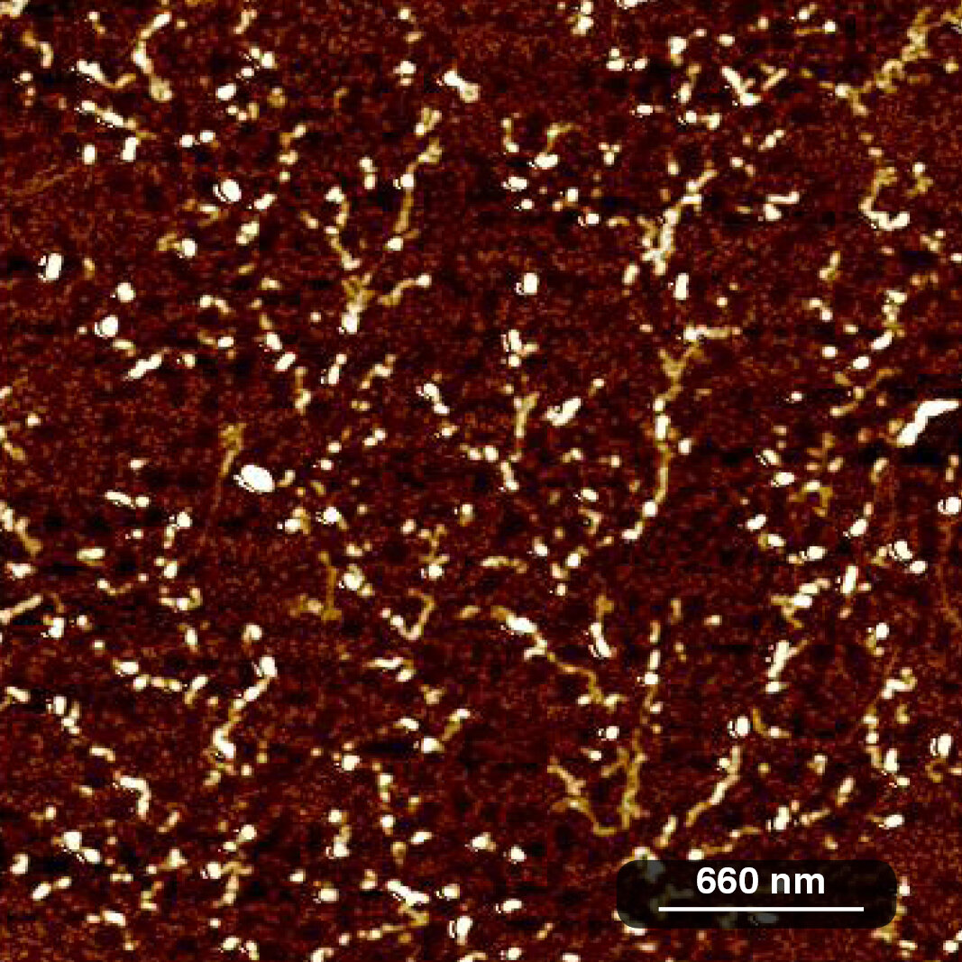
Topography image of DNA origami taken using a SCOUT 350 RAl on a Dimension icon AFM.
Image courtesy of Dr. Mark Freeley from the Queen Mary University of London.
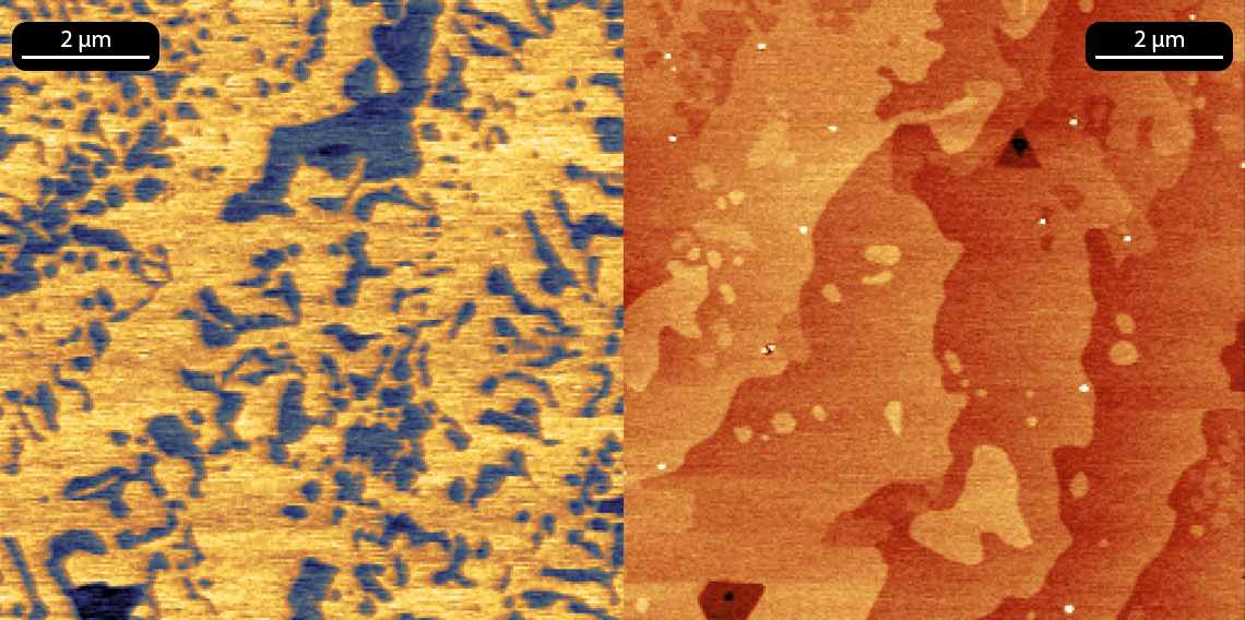
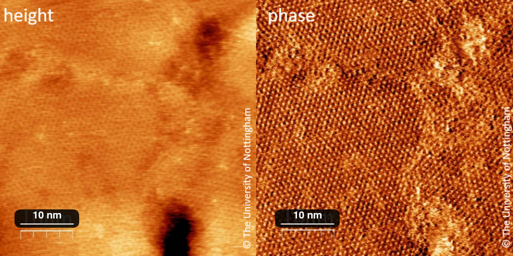
Nanostructured polymer film height (left) and phase (right) images. The phase image correlates the height difference to a change in the structure. Obtained using SCOUT 350 RAl in tapping mode in a Dimension 3100 AFM.
Images courtesy of Mr Daniel Kool, AG Prof. Lindner, Paderborn University
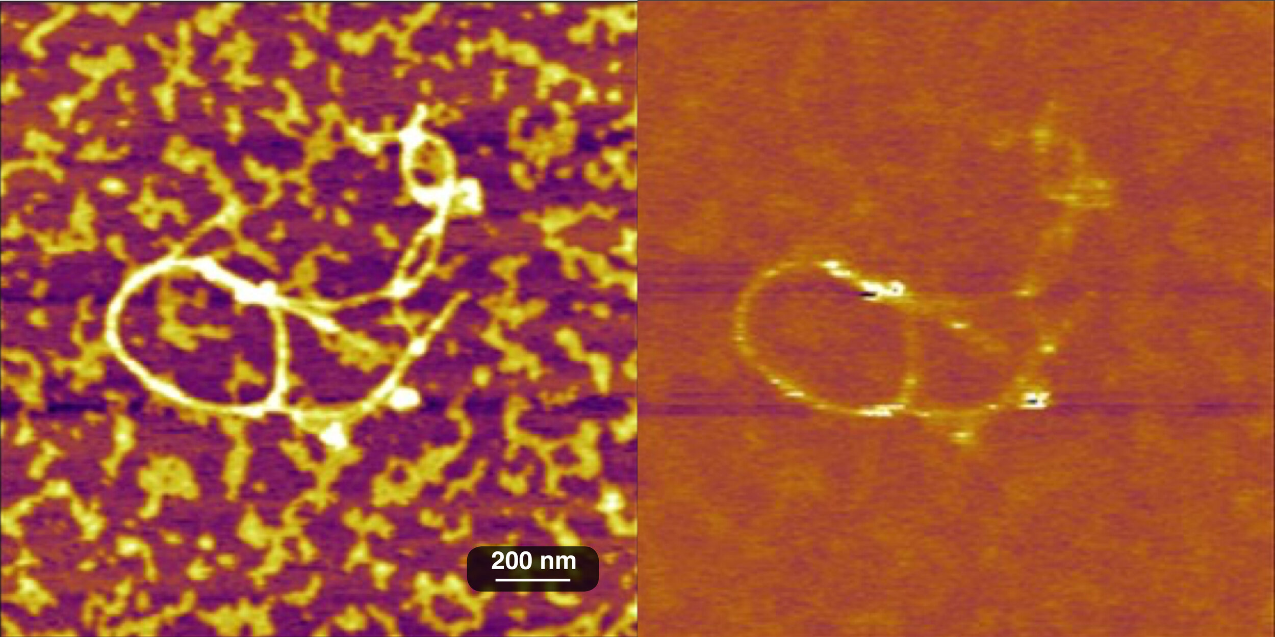
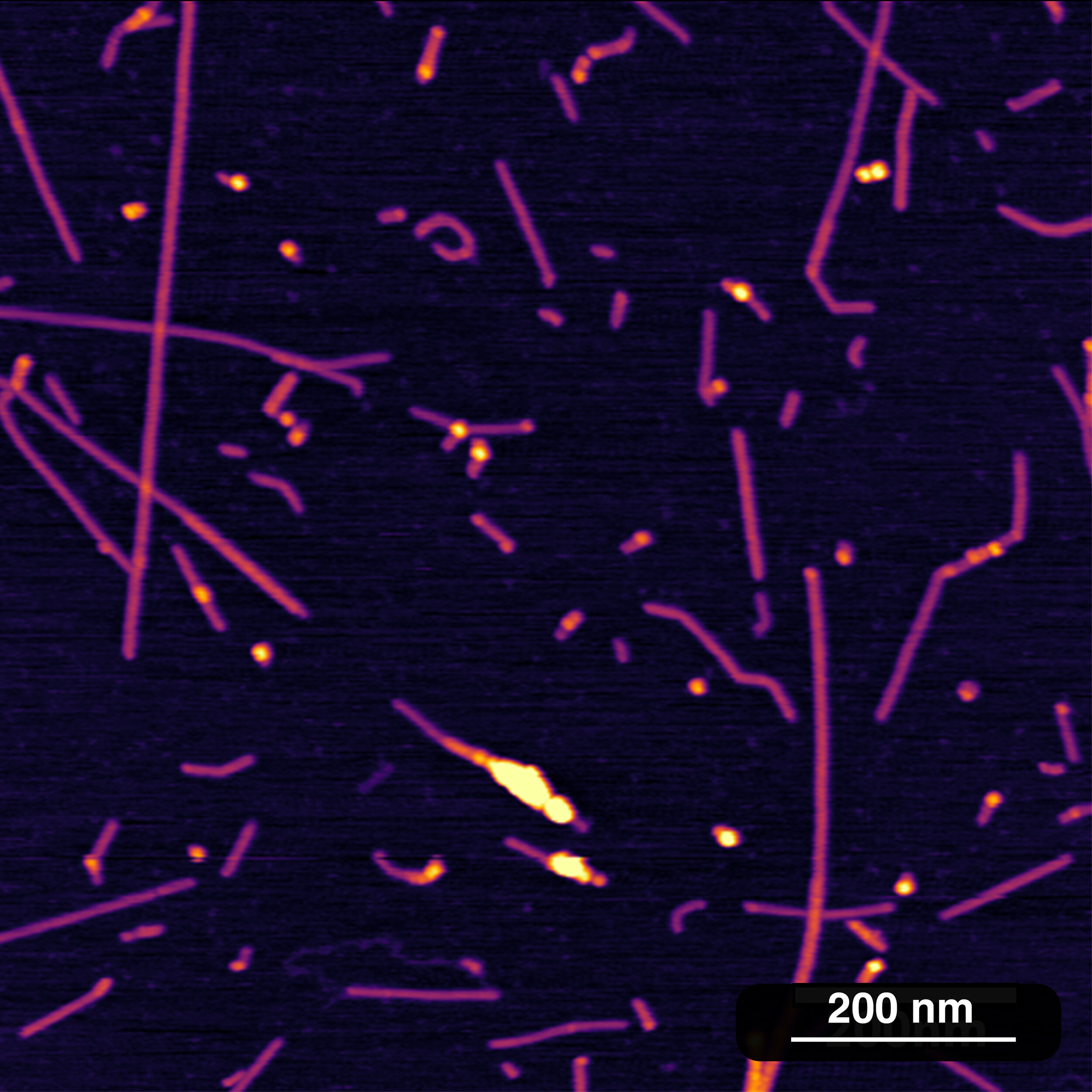
Topography image of DNA wrapped SWCNT taken with a SCOUT 70 RAu on a Bioscope Resolve AFM.
Image courtesy of Dr. Biran Wang from Memorial Sloan Kettering Cancer Centre
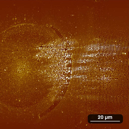
Topography image of glass lasered with several very strong laser pulses. The waves are melted glass interference of the laser. Obtained using SCOUT 350 RAl.
Image courtesy of Dr. Ladislav Fekete, Czech Academy of Science
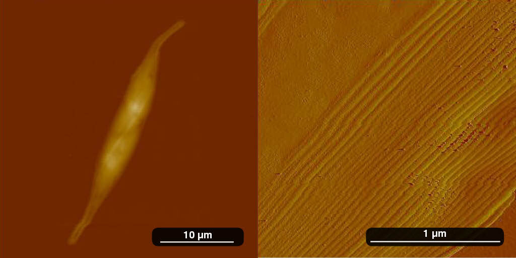
Topography microscopy images of marine microalgae Cylindrotheca sp. obtained using the SCOUT 70 RAl.
Images courtesy of Dr. sc. Tea Mišić Radić and Andrea Čačković, Mr.sc. at the Laboratory for marine and atmospheric biogeochemistry in the Ruđer Bošković Institute, Croatia.
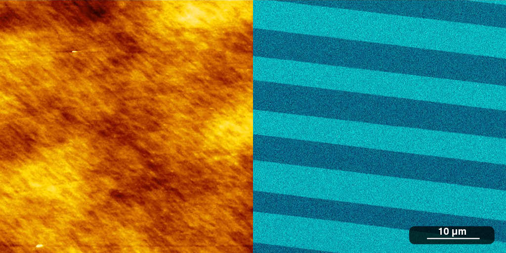
Topography and piezo-response microscopy images of a periodically poled lithium niobate surface. Acquired using a SPARK 70 Pt probe in an Hitachi automated AFM5500.
Image courtesy of Dr Colin Grant, Hitachi High Technologies Europe
Strained MBE graphene grown on hBN flakes exfoliated on a sapphire substrate (carbon aggregates across the sapphire provide a conductive substrate/connection to graphene) recorded with the NuNano SPARK 70 Pt probe. All images recorded with an Asylum Research Cypher S AFM under ambient conditions. A negative bias of -5mV was used for all images.
Image courtesy of James Thomas & Prof. Peter Beton, University of Nottingham
Insulating MgO sample, lithographically modified by trapping electrical charge using a tip bias voltage, and subsequently imaged by KPFM. Both lithography and imaging using a SPARK 350 Pt probe in an NT-MDT Ntegra AURA.
Image courtesy of Dr Héctor Corte-León, National Physical Laboratory
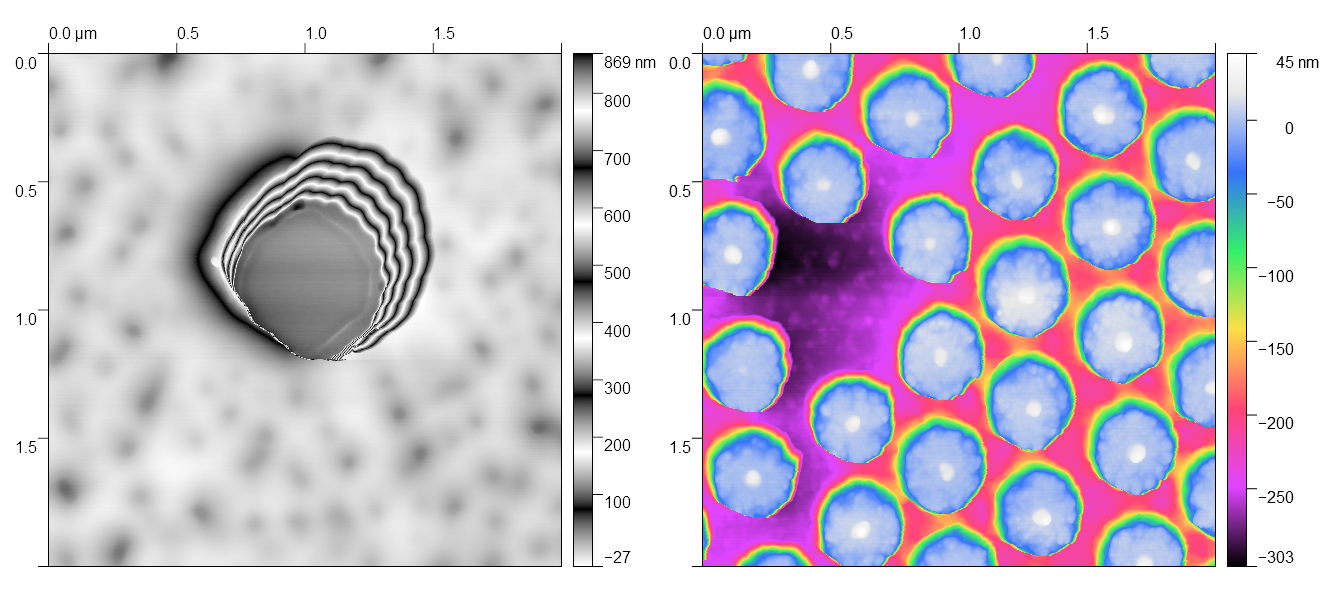
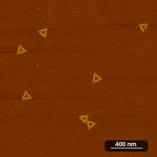
C60 nanostructures clustered on the step edges of a pentacene layer. Imaged using SCOUT 350 RAl probes in tapping mode with an Agilent SPM 5500 system. (Image size: 2 x 2 μm, z-scale: 1.5 μm) A paper has been published on this work.
Image courtesy of Ms. Andrea Huttner, Dr. Tobias Breuer, and Prof. Dr. Gregor Witte, University of Marburg, Germany.
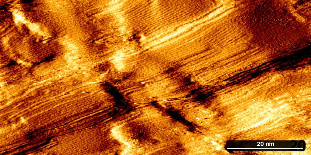
Amplitude image of plumbers PTFE tape acquired with AC mode in air using a JPK NanoWizard® Ultra and a SCOUT 70R probe.The thin features oriented from bottom left to top right are the PTFE molecules, spaced by 0.5-0.75 nm depending on the crystal orientation.
Image courtesy of Dr Nic Mullin, University of Sheffield, UK
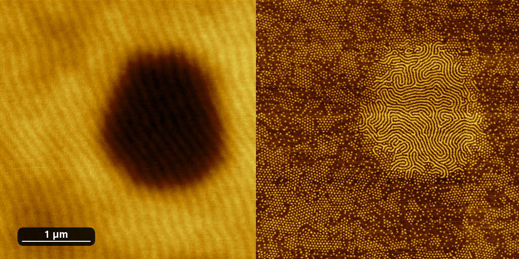
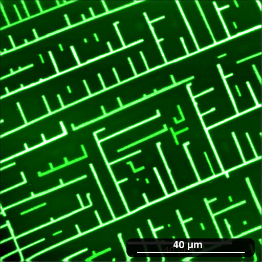
A micro-street map of self-organised microstructures on a flat substrate. The image was acquired using a SCOUT 350R AFM probe in PeakForceTapping® mode on a Bruker Multimode 8 AFM.
Image courtesy of Dr. Georg Haehner, University of St. Andrews
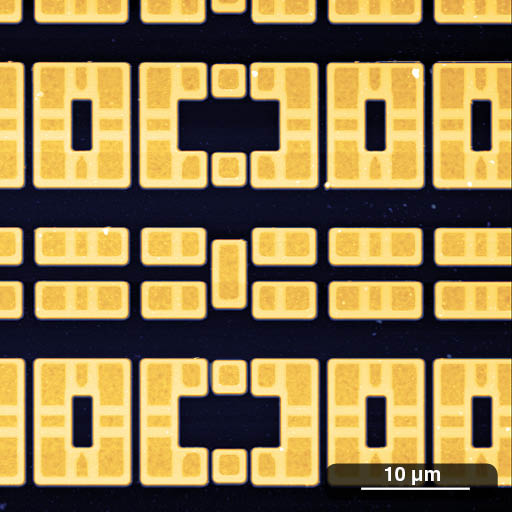
Semiconductor-processed silicon wafers with SRAM test structures. Images acquired using SCOUT 70R AFM probes in PeakForce Tapping® on a Bruker Dimension Edge AFM. (Image size: 50 x 50 μm, z-scale: 900 nm)
Image courtesy of Dr Filip Gucmann, University of Bristol, UK.
Heptacene-based island-like crystallites grown on Al2O3. Imaged using SCOUT 350 probes in AC mode with a Digital Instruments Nanoscope III AFM (Image size: 5 x 5 μm, z-scale: 10 nm)
Image courtesy of Dr Aleksandar Matkovic, Aydan Çiçek, Dr Markus Kratzer & Prof Dr Christian Teichert, Montanuniversität Leoben, Austria.
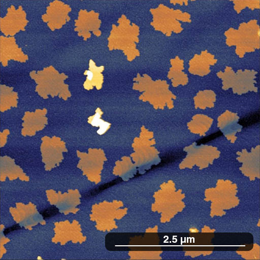
Approx 2 ML C60 on Au (111) imaged using a SCOUT 350R probe in AC (tapping) mode in ambient environment on an Asylum Research Cypher AFM.
Images courtesy of Dr Vladimir Korolkov & Prof. Peter Beton, University of Nottingham, UK.
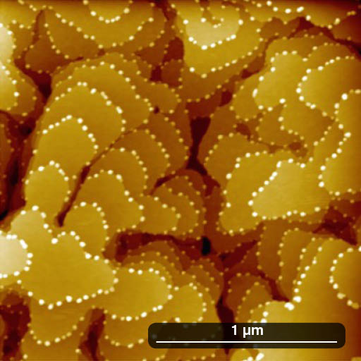
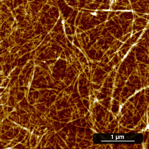
Film of cellulose nanofibrils (CNF) spin-coated onto mica. Imaged using SCOUT 350R probes in AC mode with a Bruker Multimode 8 AFM (z-scale: 50 nm).
Image courtesy of Dr Juan José Valle-Delgado, Aalto University, Finland
Connect with us to be the first to hear about news and special offers.
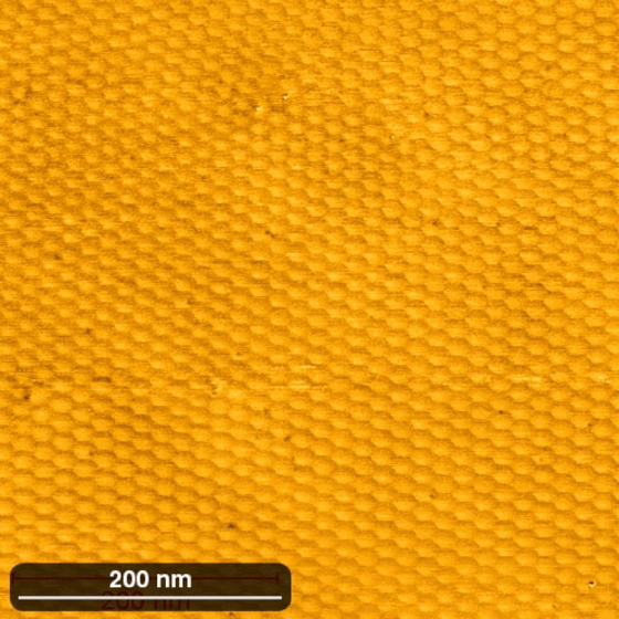
AFM imaging of hydroxyapatite crystals exposed longitudinally during enamel sample preparation using our SCOUT 350 RAu probes.
Image courtesy of Dr Sebastian Aguayo from Pontificia Universidad Católica de Chile.