

Atomic force microscopy’s (AFM) applications are wide and varied, with new modes and protocols being developed every year. But what may come as a surprise to some, is that AFM probes can be used not just for imaging surfaces, but also modifying them through techniques such as Scanning Probe Lithography (SPL).
The vision that atomic force microscopy could be used for future data storage and semiconductor fabrication applications was instrumental (no pun intended!) to my early interest in the world of AFM. Indeed, my PhD work focused on using high-speed AFM for nanofabrication, so this is a subject still close to my heart.
I don’t think AFM has yet realised that early vision, but without a doubt the field of scanning probe lithography has offered tantalising glimpses into what might be possible.
This includes the work of Dr Yu Kyoung Ryu, who we’ve recently had the privilege to talk with about her research and career. It brings back some memories!
Career Background

Dr Yu Kyoung Ryu
Ryu’s route into scanning probe lithography started during her PhD with Prof. Ricardo Garcia at Instituto de Ciencia de Materiales de Madrid (ICMM) (Consejo Superior de Investigaciones Científicas).
‘I loved microscopies (SEM, TEM, AFM…) and thought I would characterise fascinating material properties with an AFM tip. The big surprise was that my supervisor gave me the topic of using an AFM tip to fabricate optoelectronic devices at the nanoscale and high-resolution nanostructures of different materials, in my case silicon and 2D materials.
This technique is called scanning probe lithography (SPL) and comprises of a family of different modalities: oxidation, thermal, mechanical, and dip pen nanolithography to name a few. I fell in love with the technique, and it is a passion I keep up to date’.
During her PhD, Ryu participated in a European project called ‘Single nanometer manufacturing for beyond CMOS devices’. This gave Ryu the chance to meet her first postdoctoral supervisor, Dr Armin Knoll, from IBM Research Zurich, who was also involved in the project.
‘His work is focused on thermal scanning probe lithography. This modality of SPL (and atomic force microscopy itself!) was developed at IBM Zurich. It was awesome to have the opportunity to do my postdoctorate there, I have very good memories’.
At present, Ryu is a postdoctoral researcher at the Instituto de Sistemas Optoelectrónicos y Microtecnología (ISOM) in the group ‘ISOM Graphene’ under the supervision of Prof. Javier Martinez Rodrigo.
Currently and in following years, she will focus on the fabrication of energy harvesting and storage devices based on graphene and other 2D materials applying different lithographies, among them scanning probe lithography and laser writing.
AFM Probes and Scanning Probe Lithography
As is evident from Ryu’s career background, AFM probes can be used not just to image surfaces through AFM but also in techniques such as SPL to fabricate devices and materials. Ryu explained that she has experience of SPL in two modalities: oxidation and thermal.
‘In SPL, you can use your AFM tip to fabricate a structure and to inspect it. In this way, you can monitor the lithographic process while it is happening and if you see the process is not successfully occurring, you can stop it.
In the case of oxidation SPL, you put an AFM tip into contact with or a few nanometres above the sample. Then, you apply a potential between the tip and the sample and by means of the electric field, you create a water meniscus between them and produce the electrolysis of the water. The meniscus acts like an electrochemical cell at the nanoscale and the oxyanions are directed into the surface of the sample, oxidizing it. That is how oxides are created on the material.
While in the case of thermal SPL, a devoted silicon cantilever with three legs at different levels of doping was developed to heat the AFM tip. When you approach the AFM tip to a sample, by controlling the force and the temperature of this tip, you can indent/modify the surface at different sizes’.
Recent SPL Research
Ryu has contributed to several research papers throughout her career, most recently a paper studying the combination of oxidation scanning probe lithography (o-SPL) and oxygen plasma to fabricate nanoribbon field-effect transistors and nano-constrictions on few-layer MoS2 and MoSe2 (1).

Oxidation SPL on few-layer MoS2 and MoSe2 (Ryu et al., 2021).
‘The process involved using oxygen plasma to first form a thin, uniform oxide layer on top of the flake surface. This enabled o-SPL nanopatterning with full control of shape and size using n+-doped silicon AFM probes. Secondly, oxygen plasma was used to thin down the flake.
Since plasma-based and o-SPL oxides are soluble in deionised H2O, this allowed etching and the definition of electrically isolated sub-10 nm wide nano-constrictions and nanoribbon transistors’.
We were also keen to find out from Ryu which pieces of research she was most proud of and why, particularly as she has experience of SPL in several modalities.
‘In oxidation SPL, I am proud of how we developed the combination of oxidation SPL and oxidation by oxygen plasma to develop the fabrication of nanoribbons channel field-effect transistors based of transition dichalcogenide thin layers (1,2).
In thermal SPL, we achieved an array of silicon nanowires 7 nm wide and I participated in the fabrication of the first devices made using the mix and match lithography tool (thermal SPL and laser writing) developed at IBM Zurich. This result is key because this hybrid lithography strategy means a solution to low throughput inherent to the SPL technique (3,4)’.
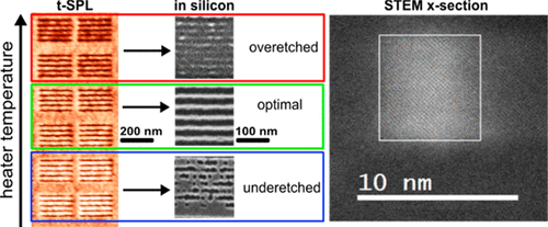
Study of the transfer reliability and the achievable resolution of thermal SPL as a function of applied temperature and force, and a scanning transmission electron microscopy (STEM) x-section of SiNW which is approximately 7 nm wide (Ryu et al., 2017).
Scientific Development and SPL
At NuNano we would like to see the AFM and associated scientific communities grow, but for that to happen new scientists need to learn about and apply these techniques to their future research. With Ryu’s experience in using techniques such as SPL, we wanted to find out why she thought it was important for early career research scientists to get involved with SPM/AFM/SPL for the future of science.
‘A single characterization tool cannot provide all the information you need to understand and solve a scientific problem. In the same manner, a single lithographic tool cannot fabricate all the components needed to achieve a functional and high-performance device.
Without SPM/AFM/SPL techniques it may be difficult to unravel some specific problems, particularly because they have a high-resolution capability and a versatility that often cannot be outperformed by other techniques. Therefore, there is a continuous need for scientists to keep alive the knowledge and further development of the SPM/AFM/SPL fields’.
If you would like to connect with Yu Kyoung Ryu or learn more about her work, please check out her LinkedIn, Twitter, Google Scholar or Researchgate profiles.
Below are a selection of publications Ryu has contributed to:
Ryu, YK., Dago, AI., He, Y., Espinosa, FM., López-Elvira, E., Munuera, C. and Garcia, R. (2021). 'Sub-10 nm patterning of few-layer MoS2 and MoSe2 nanolectronic devices by oxidation scanning probe lithography'. Applied Surface Science, 539, 148231. DOI: 10.1016/j.apsusc.2020.148231
Dago, AI., Ryu, YK., Palomares, FJ. and Garcia, R. (2018). 'Direct patterning of p-type-doped few-layer WSe2 nanoelectronic devices by oxidation scanning probe lithography'. ACS Applied Materials & Interfaces, 10(46), 40054-40061. DOI: 10.1021/acsami.8b15937
Rawlings, CD., Ryu, YK., Rüegg, M., Lassaline, N., Schwemmer, C., Duerig, U., Knoll, AW., Durrani, ZAK., Wang, C., Liu, D. and Jones, ME. (2018). 'Fast turnaround fabrication of silicon point-contact quantum-dot transistors using combined thermal scanning probe lithography and laser writing'. Nanotechnology, 29(50), 505302. DOI: 10.1088/1361-6528/aae3df
Ryu, YK., Rawlings, C., Wolf, H., Spieser, M., Bisig, S., Reidt, S., Sousa, M., Khanal, S., Jacobs, T. and Knoll, AW. (2017). 'Sub-10 nanometer feature size in silicon using thermal scanning probe lithography'. ACS Nano, 11(12), 11890-11897. DOI: 10.1021/acsnano.7b06307
If you enjoyed this blog post, you might also like Women in STEM: An Interview with Becky Sage, CEO of Interactive Scientific or Women in STEM: An interview with Hannah Levene, NuNano Process Engineer.

We’re always looking for new women to interview from the AFM field, so please email us at community@nunano.com if you have any recommendations!